TECHNOLOGY
microLED light source

TECHNOLOGY

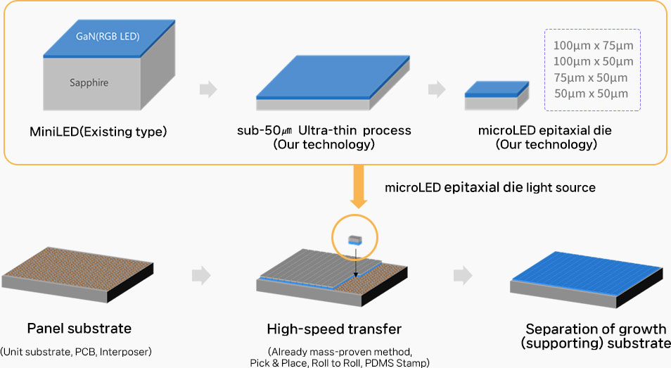
Relatively large MiniLED light source is manufactured using conventional transfer method on PM-driven PCB
(issues raised with microLED light source size reduction and productivity)

Manufacturing ultra-small & ultra-miniature microLED light source on AM-driven TFT backplane using challenging transfer process
(issues raised with the requirement of 100% light source electro-optic characteristic yield and defect countermeasure)

· Use of only measured and classified
good quality light sources
· Use of already proven transfer technology
· SSeparation of growth (supporting) substrate
by LLO technology
· MiniLED ultra downsizing
Microdisplays are a core technology for metaverse devices, still under development with many technical obstacles.
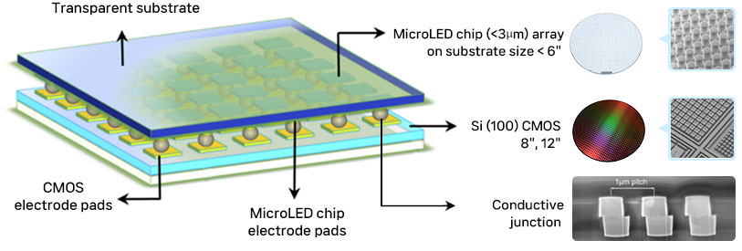
· 8" and larger large diameter RGB
epitaxial wafer issues
· 8" and larger engineered monolithic
epitaxial wafer issues
· Chip downsizing issues
(performance degradation, manufacturing process complexity)
· Chip bonding issues
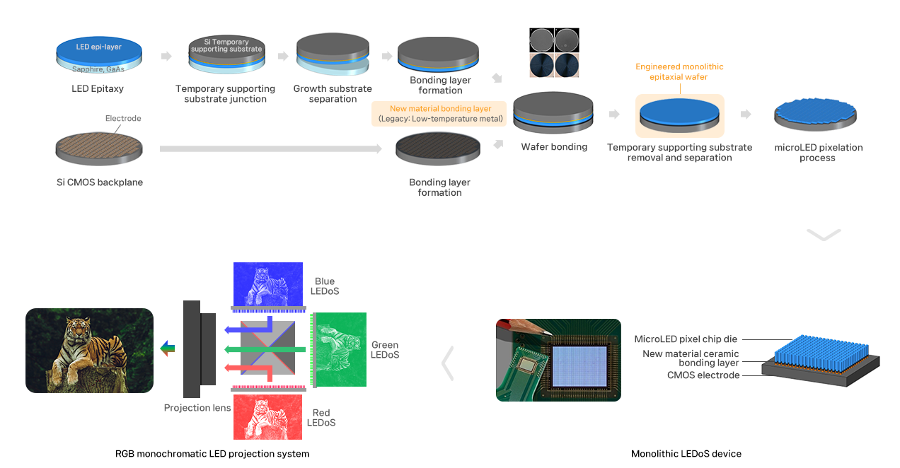
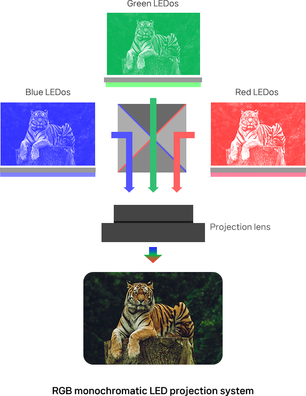
· RGB Color
(Color Conversion or Blue-Green-Red
array)
By using new material ceramics instead of opaque metal bonding layers, we provide solutions that address key technical issues


WaveLord Inc. is the only SME in South Korea that can provide microLED light sources
by establishing fab & chip die process facilities in addition to GaN epitaxy facilities
▶ Provides microLED light source and foundry services to industry, academia and research institutes developing microLED displays
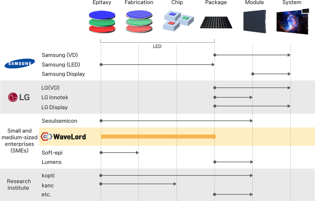
microLED light source & Power Semiconductors

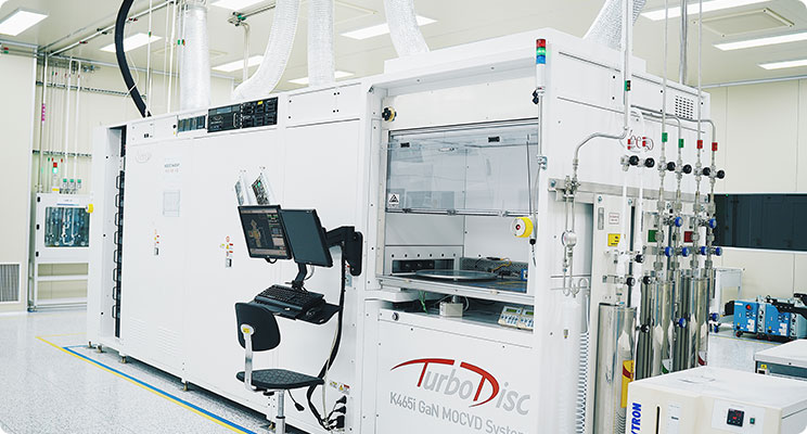
MOCVD : 3(K465i 2, HT-Crius 1)
Analysis equipment : XRD, PL(266nm), PL(375nm), Quick-EL, AFM, Normalski OM
COW, COT, Epitaxy die , Engineered Monolithic epitaxial wafer
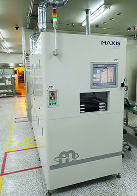
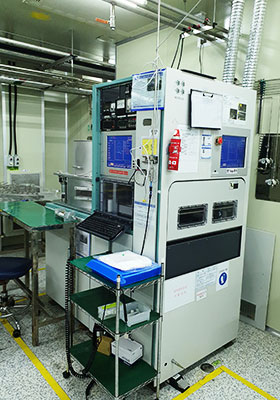
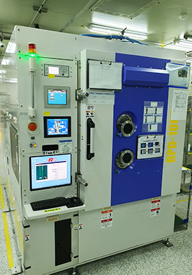

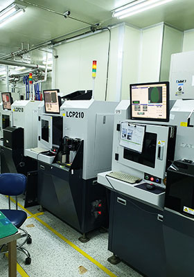
Fab : Photolitho Tools(Stepper, Aligner, Track) Plasma Etcher, CVD, PVD, RTA
Chip : Lapping, Polishing, Probe
Evaluation analysis : Microscope, SEM, Integrating sphere